


Coherent Control of the Hartman Effect through a Photonic Crystal with Four-Level Defect Layer
Cite this Article
Hu Feng-Lian, Badshah Fazal, Basit Abdul, Zhang Hai-Yang, He Qing, Ge Guo-Qin. Coherent Control of the Hartman Effect through a Photonic Crystal with Four-Level Defect Layer. Communications in Theoretical Physics, 2018, 70(5): 613 
Permissions
Coherent Control of the Hartman Effect through a Photonic Crystal with Four-Level Defect Layer
† Corresponding author. E-mail:
Supported in part by the National Natural Science Foundation of China under Grant Nos. 11274132 and 11750110411
Abstract
Abstract
In this paper, we examine the transmission of a probe field through a one dimensional photonic crystal (1DPC) when the sixth layer of the crystal is doped with four level atoms. We analyze effects of the external driving field on the passage of weak probe field across the photonic crystal. It is found that for the phase time delay of the probe photons, intensity of the driving field switches the Hartman effect from sub to superluminal character. It is interesting to note that in our model, the superluminal transmission of the probe pulse is accompanied by a negligibly small absorption of the incident beam. It ensures that the probe field does not attenuate while passing through the photonic crystal. A similar switching of the Hartman effect may be obtained by adjusting detuning of the probe field related to the excited states of the four-level doping atoms.
1 Introduction
Photonic crystals (PCs) are periodic dielectric media with some exceptional electromagnetic (EM) properties. The most striking feature of these materials is their band-gap structure (BGS) commences due to the interference of light (i.e., Bragg scattering). Within the photonic band gap (PBG) the electromagnetic field is evanescent. Such an evanescent EM field has an analogy with the electrons in quantum barriers. Therefore, the one-dimensional photonic crystals (1DPCs) act as optical barriers for investigating the tunneling time of the EM signals.[1–2] The tunneling time of a particle through a barrier or the EM wave through an evanescent region has been defined in many ways.[3–8] Amongst all, phase time is the most established both theoretically and experimentally.[9–17] It represents time of traversal of the wave packet through the interaction region and is calculated by employing the energy derivative of the phase of the transmission amplitude. Here we addressed the tunneling time of probe field (photons) through a 1DPC while the tunneling of ultracold atoms (particles) and their superclassical transmission has been studied in some interesting studies.[18–19]
In recent years, the tunneling of EM waves through 1DPCs has attracted many groups of the researchers. This multi-layered arrangement has novel applications in the field of light-matter interaction.[1–2, 20–22] According to the Hartman discovery, for long enough barriers, the tunneling time becomes independent of the barrier’s length.[4] It implies superluminal and arbitrarily large group velocities inside long barriers. Since after its recognition, this important effect has been studied extensively in many different systems.[23] The presence of a defect layer in 1DPCs facilitates in providing a coherent control of the Hartman effect of the probe light by controlling susceptibility of the doping atoms in the defected layer. Similarly, the superluminal transmission of the probe field through 1DPCs for two and three level atomic doping have been analyzed in some interesting studies.[24–25] In a recent study, the effects of phase control on the Hartman effect was discussed in the presence of multiple driving fields.[26]
Atomic coherence and quantum interference play a crucial role in controlling the absorption and dispersion nature of the atomic media. In this scenario, the double electromagnetically induced transparency in an inverted-Y-type atomic system with Zeeman sublevels was investigated where it was found that the Zeeman degeneracy of the dark states may be lifted by the increasing intensity of the dressing field.[27] Similarly, the laser-induced atomic gratings may be used to study various characteristics of the stable multicomponent vector solitons consisting of two perpendicular four-wave mixing (FWM) dipole components.[28] Likewise, Zhang et al. experimentally studied PT-symmetric optical lattices with controllable gain-to-loss ratio in a coherently prepared N-type atomic ensemble. The relevant index modulation and the antisymmetric gain and loss profiles were introduced by exploiting the modified absorption and Raman gain in the four-level atomic configuration.[29] Further, interference of the three coupling fields have been used for splitting energy levels periodically, to form a periodic refractive index structure with honeycomb profile that can be adjusted by the system’s controlling parameters.[30]
Modification of the absorption and transmission characteristics of the atomic medium due to the quantum coherence and interference may lead to the subluminal and superluminal light propagation. It is quite well known that the super and subluminal propagations of light are due to the anomalous and normal dispersions, respectively.[31–33] It has been shown that for anomalous dispersions the group velocities of EM pulses may be abnormal, i.e. greater than c (the speed of light in vacuum), or even becomes negative.[32,34] It has many potential applications in various fields like the all-optical routing,[35–36] all-optical switching,[37] optical memories, and interferometry.[38–39] Here we use intensity of the external driving field to change the dispersion and absorption properties of 1DPC, which further control the phase time delay and the Hartman effect related to the probe field transmission.
In this paper, we study transmission of the probe field through a one-dimensional photonic crystal. We consider that the sixth layer of the photonic crystal serves as a defected layer due to the doping of four-level atoms, which modifies response of the medium to the incident probe field in a similar fashion to the earlier studies related to the absorption and dispersion characteristics of the atomic media.[27–30] By analyzing the tunneling time of transmission, we find that a superluminal propagation of the probe field may be obtained by controlling intensity of the external driving filed. It is noted that the phase time delay saturates with the increasing stack number of the photonic crystal and thus the Hartman effect may be realized for the probe field propagation. Our results show that a proper adjustment of the driving field provides a switching of the Hartman effect from sub to superluminal character. It is interesting to note that here the superluminal transmission of the probe pulse is obtained for a negligible absorption of the probe field, which is always desirable in an experimental treatment. In addition, we show that detuning of the probe field also affects behavior of the phase time delay and causes a switching of the Hartman effect from positive to negative values.
2 Model and Dynamics
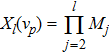
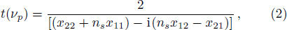
1 ) nj is a function of νp and represents the refractive index of the j-th layer. The transmission coefficient 


Our model consists of a one-dimensional photonic crystal made up of dielectric layers with structural sequencing as (ab)NL a. Here the symbols “a” and “b” are the two different layers of the dielectric material. We take “a” to be the titanium oxide with an index of refraction na = 2.22, while “b” is the fused silica with an index nb = 1.41. The notation NL stands for the stack number which gives periodicity of the 1DPC and is a measure of its length. The two types of layers satisfy the condition nada = nbdb = λ0/4 i.e. they have equal optical thickness. Here λ0 is the mid-gap wavelength of the probe field which we have taken as 692 nm, while ω0 = 2πc/λ0, is the corresponding frequency with c being the speed of light in free space. The over all structure of the 1DPC is characterized by the sequence of layers (ab)2 aD(ab)NL a with D as the defected layer doped with four-level atoms.
Here our aim is to analyze propagation of the probe field through the 1DPC whose sixth layer is doped with a four-level atomic system as shown in Fig.
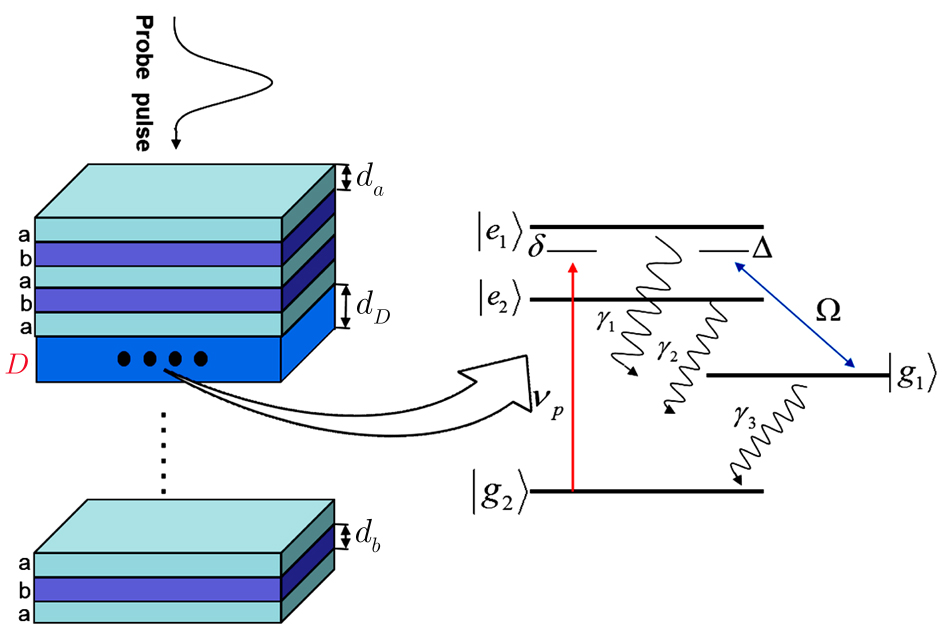 | Fig. 1 (Color online) Schematics of the 1DPC with defect layer. The level structure shows an EIT configuration of the atoms doped in the defect layer D. |
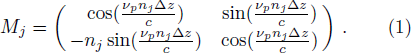
There is vacuum at the two ends of the 1DPC and a normal incidence of the probe field is considered for its transmission through the crystal. Using the transfer matrix approach, the electric and magnetic field components at the two nearby positions z and z + Δz in a certain layer can be found as[24]

In order to analyze the probe field transmission, we must have an explicit expression for the susceptibility χ of the atomic system, which gives the steady state response of the atoms to the applied field. Solving the density matrix equations of motion at the steady state lead to the dispersion and absorption spectra, which are determined by the real and imaginary parts of the susceptibility[43]
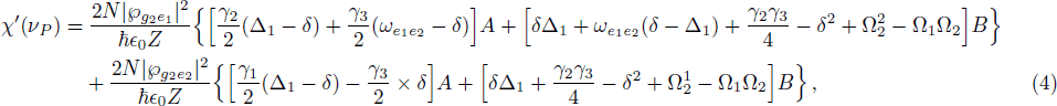
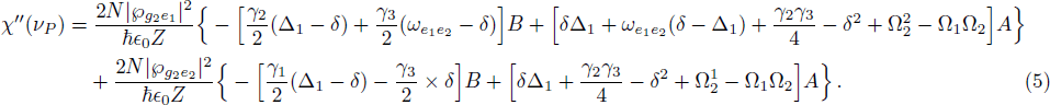


The dielectric function of the doped layer D can be defined as ϵ(ω) = ϵB + χ, where 
3 Results and Discussion
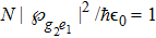
For our numerical results, we assume 
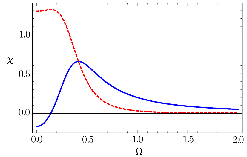 | Fig. 2 (Color online) Real (solid curve) and imaginary (dashed curve) parts of the susceptibility (χ) as a function of the driving field Ω for δ = 0 and Ω1 = Ω2 = Ω. Other parameters are γ1 = γ2 = 3γ, γ3 = 0, Δ1 = 0.2γ, ωe1e2 = 0.4γ. |
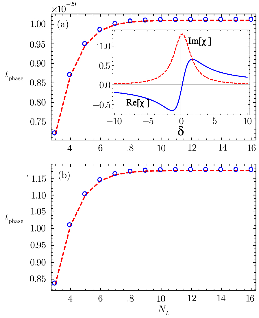
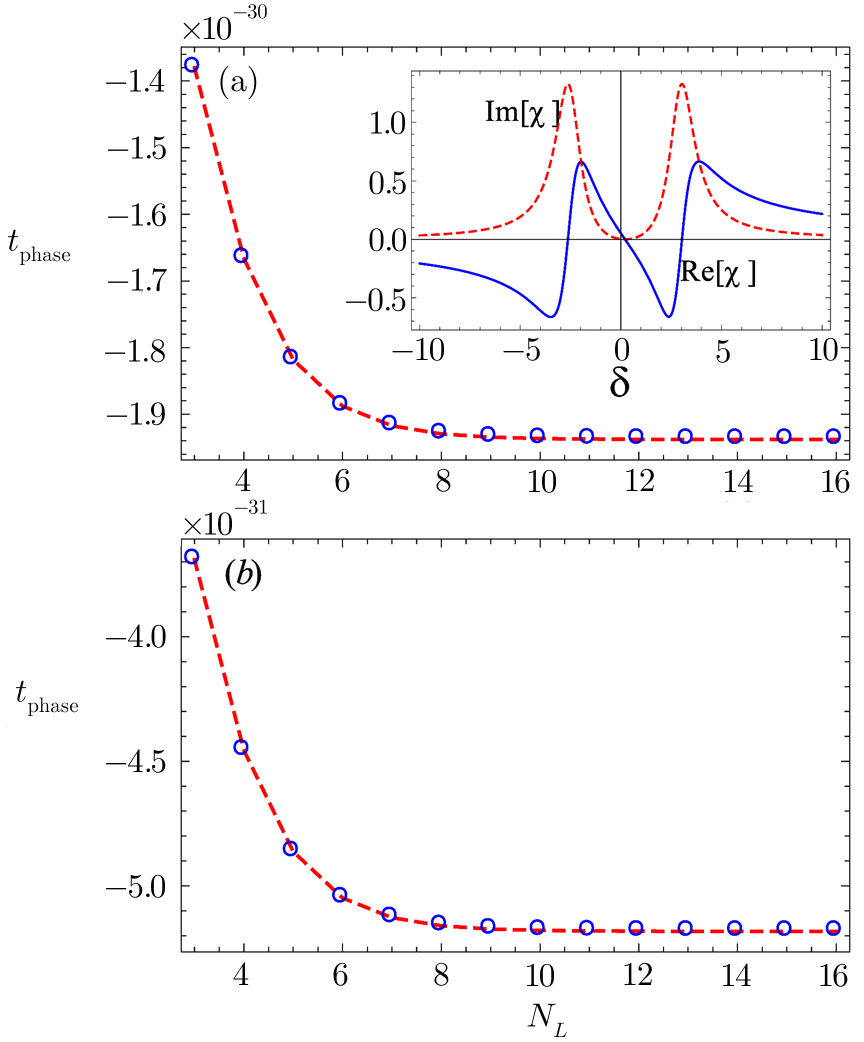
 | Fig. 3 (Color online) Phase time delay tphase vs. number of stack NL for (a) Ω1 = Ω2 = 0, (b) Ω1 = Ω2 = 0.02γ. Other parameters are γ1 = γ2 = 3γ, γ3 = 0, Δ1 = 0.2γ, ωe1e2 = 0.4γ. |
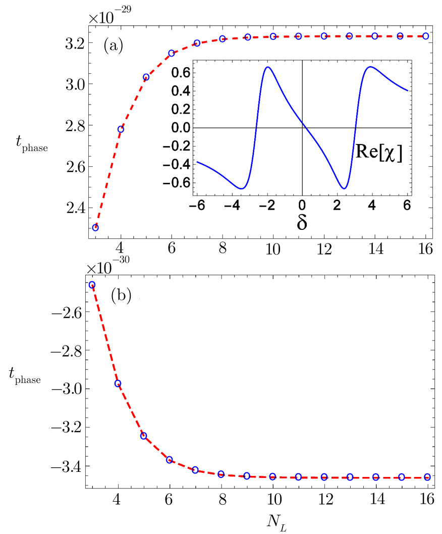
When we further increase the applied driving field to a strength Ω1 = Ω2 = 2γ, anomalous dispersion at δ = 0 is obtained as shown by the real component of susceptibility (Re[χ]) in the inset of Fig.
 | Fig. 4 (Color online) Phase time delay tphase vs. number of stack NL for (a) Ω1 = Ω2 = 2γ, (b) Ω1 = Ω2 = 4γ. Other parameters are γ1 = γ2 = 3γ, γ3 = 0, Δ1 = 0.2γ, ωe1e2 = 0.4γ. |
Further, we show a switching of the Hartman effect from sub to superluminal character by the atom-field detuning for a constant driving field (Ω1 = Ω2 = 2γ). In Fig.
 | Fig. 5 (Color online) Phase time delay tphase vs number of stack NL for the parameters in Fig. |
In summery, here we have proposed a scheme in which an incident probe field interacts with a 1DPC having a defect layer due to four-level atomic doping. The photonic crystal is made up mainly of two positive index materials with a slight doping in the sixth layer of the multi-layered arrangement. This causes a remarkable change in the dispersion and absorption characteristics of the photonic crystal. Here we find that by controlling the Rabi frequency of the external driving field one can change the phase time delay of the probe field from sub to superluminal behavior. It is noted that for a suitable values of the parameters the superluminal character of Hartman effect may be obtained for a negligible absorption of the incident beam, which is always desired in an experimental treatment. The probe field detuning also provides a switching of the Hartman effect from positive to negative nature.
Reference
| [1] | |
| [2] | |
| [3] | |
| [4] | |
| [5] | |
| [6] | |
| [7] | |
| [8] | |
| [9] | |
| [10] | |
| [11] | |
| [12] | |
| [13] | |
| [14] | |
| [15] | |
| [16] | |
| [17] | |
| [18] | |
| [19] | |
| [20] | |
| [21] | |
| [22] | |
| [23] | |
| [24] | |
| [25] | |
| [26] | |
| [27] | |
| [28] | |
| [29] | |
| [30] | |
| [31] | |
| [32] | |
| [33] | |
| [34] | |
| [35] | |
| [36] | |
| [37] | |
| [38] | |
| [39] | |
| [40] | |
| [41] | |
| [42] | |
| [43] | |
| [44] | |
| [45] |