


Ti Impurity Effect on the Optical Coefficients in 2D Cu2Si: A DFT Study
Cite this Article
Nourozi Bromand, Boochani Arash, Abdolmaleki Ahmad, Sartpi Elmira, Darabi Pezhman, Naderi Sirvan. Ti Impurity Effect on the Optical Coefficients in 2D Cu2Si: A DFT Study. Communications in Theoretical Physics, 2018, 69(1): 101 
Permissions
Ti Impurity Effect on the Optical Coefficients in 2D Cu2Si: A DFT Study
† Corresponding author. E-mail:
Abstract
Abstract
The electronic and optical properties of 2D Cu2Si and Cu2Si:Ti are investigated based on the density functional theory (DFT) using the FP-LAPW method and GGA approximation. The 2D Cu2Si has metallic and non magnetic properties, whereas adding Ti impurity to its structure changes the electronic behavior to the half-metallic with 3.256μB magnetic moment. The optical transition is not occurred in the infrared and visible area for the 2D Cu2Si in x-direction and by adding Ti atom, the real part of dielectric function in the
1 Introduction
The amazing electronic behavior of graphene leads to a high mobility concluding from the hexagonal sheet structure.[1] Considering the Dirac cone graphene materials, several electronic and spintronic behaviors[2–5] such as ballistic charge transport,[6] high mobility,[7] and quantum Hall effects[8] are appeared. According to some restriction in carbon graphenes, many 2D materials are synthesized and predicted such as Silicene, Germanene,[9] and Ti2B.[10] It is reported that 2D materials with the honeycomb structure have different physical behaviors than those in bulk phase.[11] Hence, it is necessary to find a new class of 2D materials with new electronic, magnetic and optical properties to use in some industrial applications such as optoelectronic, spintronic, and solar cell devices.
After discovery of graphene,[12] new 2D materials have been considered such as BN,[13, 14] tertialy B-C-N,[15] etc. These 2D materials have more unique physical properties than carbon graphene and are very attractive in the electronic and optoelectronic industries. Most of the 2D chemical and physical structures have tri-coordinated motifs, as their graphene structures are illustrated,[16–22] so only a few samples of these materials have been reported by quasiplanar tetra coordinated structure. Hoffman et al., were the first group reporting 
In recent years, making planar hyper coordinate 2D materials has been a big challenge as their compound elements do not mach. The planar hyper coordinate molecules were firstly predicted by Schleger et al.,[24] a class of materials, which are very interesting in scientific and industrial points of view, and also B2C monolayer in the quasi planar hexa-coordinate carbon shape has been recently investigated.[25]
Due to the transition metals applications in the electronic industry, they are even more attractive. The 2D materials based the Cu atom have the interesting electronic and optical treatment. Recently, 2D Cu2Si has been synthesized by laying down the Cu cluster on Si (111),[25] also, as well as ab-initio calculations indicated the good stability of this 2D material. The electronic calculations by Yang et al..[26] have shown the metallic behavior for the 2D Cu2Si. Furthermore, this 2D material has strong chemical bonding between atoms and high implant stiffness. The optical properties of the 2D Cu2Si have been less considered so far, and also according to the metallic behavior of the 2D Cu2Si, it is expected that by absorbing Ti to its structure, the electronic and the optical properties of the 2D Cu2Si:Ti have been improved for optoelectronic and solar cell applications.
Since Ti belongs to the transition metals, there is a good compatibility between its electronic structure and Cu atom, thus Ti is placed instead of Cu in the 2D Cu2Si. By doping Ti into the 2D Cu2Si, the electronic and the optical properties are changed significantly. Additionally, it is noticeable that by adding Ti, magnetic behaviors emerge in the 2D Cu2Si:Ti especially at the Fermi level. In Sec.
2 Computational Methods
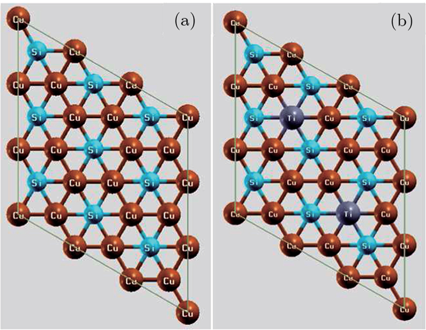
Calculations are based on the density functional theory (DFT) framework and the FP-LAPW method with the GGA approximations.[27–29] After optimization of the input parameter, the RKmax, Gmax, and KPoint are selected as 8.0, 13.0, 5000, and 8.0, 13.5, 500 for the pure and the impurity cases respectively. The lattice parameters of the 2D Cu2Si hexagonal super lattice are set to a = b = 23.374 (Bohr) and c = 18.897 (Bohr). The structures are relaxed by miniposition command with 1.0 a.u./dyne accuracy, and the optical calculations are performed by the RPA approximation.[30] For better comparison, the 2D Cu2Si and the 2D Cu2Si:Ti shapes are shown in Fig.
 | Fig. 1 (Color online) (a) The 2D Cu2Si structure, (b) The 2D Cu2Si:Ti lattice by XCrysden code. |
3 Results and Discussion
3.1 Electronic and Magnetic Properties
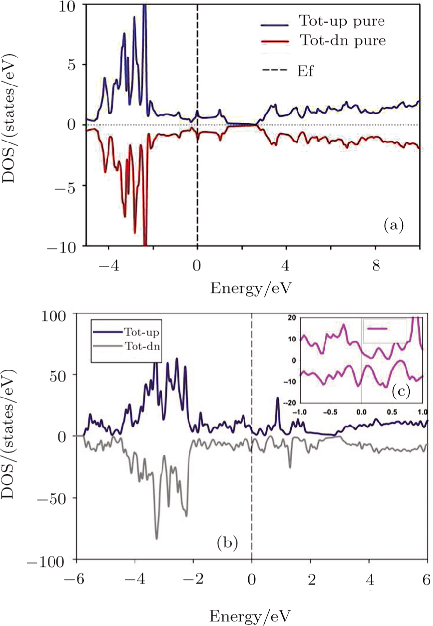
According to the other studies, the 2D Cu2Si has not good metallic treatment due to a few electron states at the Fermi level and lack of the magnetic property.[25–26] In the electronic discussions, the DOS diagram shows important information about metallic or non-metallic and magnetic or non-magnetic properties of matter. Figure
 | Fig. 2 (Color online) (a) Total 2D Cu2Si DOS versus energy, (b) Total 2D Cu2Si:Ti DOS versus energy, (c) Total DOS of 2D Cu2Si:Ti at Fermi area. |
Considering Ar3 

| Table 1
The bond length of 2D Cu2Si in pure and impurity cases (Å) with Cohesive energy (Ec), Atomic bond length (Å) and Total magnetic moment ( |
3.2 Optical Properties
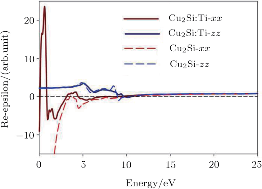
The optical properties are described by the response of matter to incident light leading to the electronic structure such as the energy band gap, the conductivity, the semiconductor behavior and the glassiness. The 2D Cu2Si and Cu2Si:Ti have two symmetric directions x and z, where x is on the plane of the structure and z is perpendicular to it. The real part of the dielectric function 


 | Fig. 3 (Color online) Real part of dielectric function for x and z directions for 2D Cu2Si and 2D Cu2Si with Ti impurity versus photon energy. |
The Real part of dielectric function 


A quick look at the 


It is noticeable that 


The 


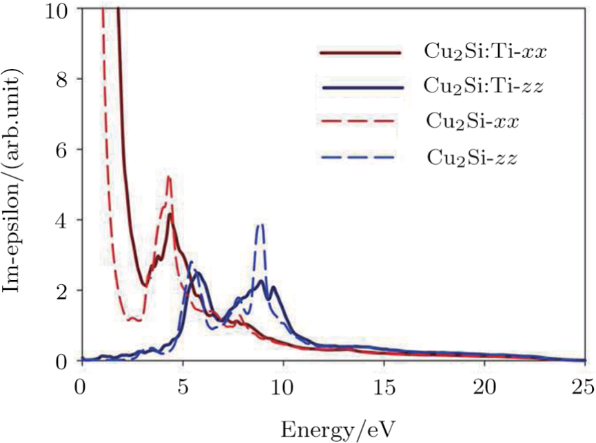 | Fig. 4 (Color online) The Imaginary part of dielectric function of 2D Cu2Si & 2D Cu2Si:Ti versus photon energy in the x & z directions. |
Afterward, the second main peak of 

The 


It is noticeable that the all 


The energy loss function diagram (Eloss) involves important information about the optical properties such as absorption, refraction and Plasmon frequency. Figure 


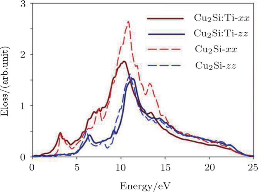 | Fig. 5 (Color online) Eloss function of 2D Cu2Si and (:Ti) cases versus photon energy in x and z directions. |
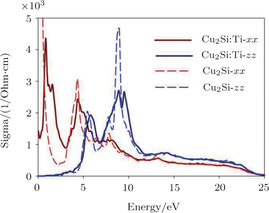
The optical conductivity is resulted from the electron transitions to the conduction bands caused by the incident radiation to matter including the important electronic and the optical information about the material. The optical conductivity in the x and z directions are in agreement with the above discussions. The optical conductivity of the 2D Cu2Si in the x and z directions are shown in Fig.
 | Fig. 6 (Color online) 2D Cu2Si, 2D Cu2Si:Ti conductivity in x and z directions versus photon energy. |
Figure 

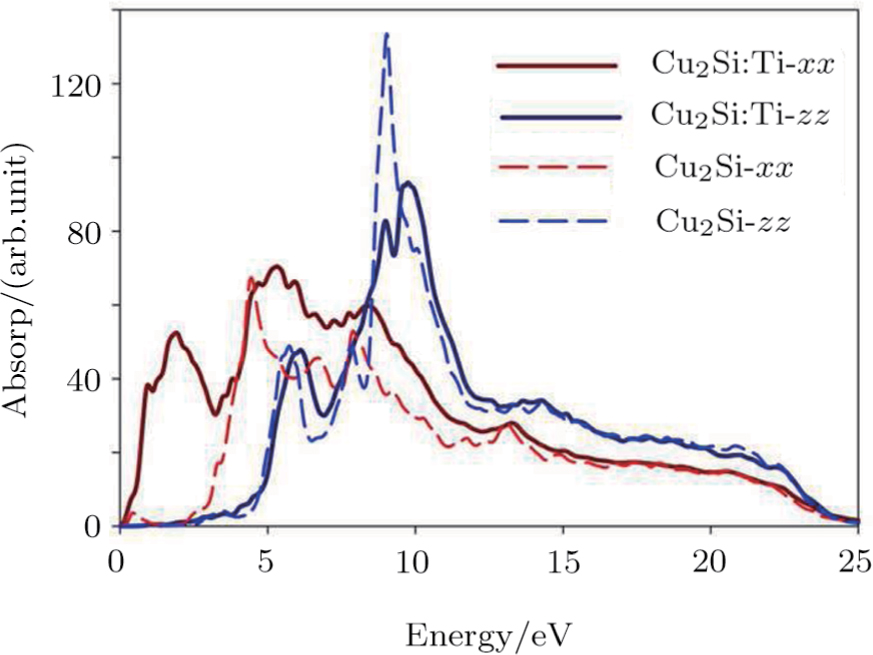
The absorption peaks of the 2D Cu2Si are presented in Fig.
 | Fig. 7 (Color online) Absorption function of 2D Cu2Si in pure and impurity cases versus photon energy in the in-plane and normal directions. |
The 2D Cu2Si:Ti absorption diagram in the x and z directions are shown in Fig. 

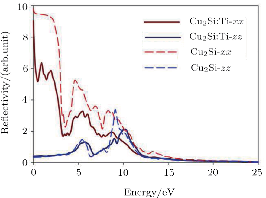
Reflection parameter is an important optical parameter for matter representing the percentage of the light transmission and reflection in the material surfaces; metals have high reflection (about 90%), for example shining matters and non-metals are opaque. The 2D Cu2Si has complete reflection at zero energy in the x direction, but it is nearly zero for the z direction indicating the different behaviors for the two mentioned directions so that the light is fully transmitted in the direction perpendicular to 2D Cu2Si surface, and completely reflected in the coplanar state. By increasing the photon energy, the reflectivity in the z direction is dropped significantly at 3.5 eV (the visible area) to reach its second maximum at 4.7 eV. Figure
 | Fig. 8 (Color online) Reflection index of 2D Cu2Si & 2D Cu2Si:Ti versus photon energy in x & z directions. |
It is clear that the static amount of the reflection for the 2D Cu2Si:Ti in the x direction is 90% confirming its metallic behavior, whereas this compound shows the semiconductor behavior in the z direction due to a low static reflectivity (Fig. 
4 Conclusion
In summary, calculations of the Ti impurity effect on the 2D Cu2Si are performed based on the DFT framework by the GGA approximation. In the pure case, the DOS diagrams cut the Fermi level and do not have magnetic moment, but the 2D Cu2Si:Ti has half-metallic behavior with the magnetic moment of 
In the pure case, no optical transition occurred in the x direction in the infrared and the visible areas, but in the impurity case, it has a Dirac peak in the infrared area. The major electron transitions are occurred from the Cu-d and the Ti-d to the S-p and the Cu-d orbitals. The absorption gap is reduced to zero in the x direction and is sensitive to the incident light, but it is relatively the same in the pure and the impurity cases in the z direction. According to the Ti atomic structure, the 2D Cu2Si:Ti has lower metallicity in zero energy, whereas its optical conductivity and reflectivity are smaller than the 2D Cu2Si case.
Owing to the semi-metallic behavior of Cu2Si:Ti at the Fermi level, it is expected that this compound will be used in the spintronics and giant magnetoresistance (GMR). In addition, by adding Ti to the 2D structure of Cu2Si, the light absorption gap along xx has been vanished, and an increase in the light absorption can be observed in the infrared and visible regions making this composition suitable for solar cells and optical devices.
Reference
| [1] | |
| [2] | |
| [3] | |
| [4] | |
| [5] | |
| [6] | |
| [7] | |
| [8] | |
| [9] | |
| [10] | |
| [11] | |
| [12] | |
| [13] | |
| [14] | |
| [15] | |
| [16] | |
| [17] | |
| [18] | |
| [19] | |
| [20] | |
| [21] | |
| [22] | |
| [23] | |
| [24] | |
| [25] | |
| [26] | |
| [27] | |
| [28] | |
| [29] | |
| [30] |